What Is Characteristic Impedance?
Every transmission line has a characteristic impedance, Z₀ — the single most important number on its datasheet. It is quoted for cables (50 Ω RG-58, 75 Ω RG-6), for PCB traces ("50 Ω controlled impedance"), for differential pairs (90 Ω USB, 100 Ω Ethernet) and for antennas' feed lines. Yet it is often misunderstood, because it has units of ohms but is not a resistance you can measure with an ohmmeter.
There are three equivalent ways to define it, and each gives a different insight:
Part 3 obtained Z₀ as a by-product of solving the telegrapher's equations. This article puts it at the centre: what it means physically, how to derive it, how geometry and materials set its value, and how to measure it. For the Smith-chart view of Z₀ — as the impedance every other impedance is normalised to — see Understanding Characteristic Impedance of Transmission Lines in the Smith chart series.
Physical Meaning of Characteristic Impedance
Connect a battery to an uncharged, lossless line. A voltage step V⁺ travels down it at vp, charging the capacitance of each new metre it reaches (Part 1). To charge C′ per metre to V⁺ at vp metres per second, the battery must supply a current I⁺ = C′vpV⁺. So the battery sees a steady current proportional to its voltage — exactly as if it were connected to a resistor of value V⁺/I⁺ = 1/(C′vp) = Z₀.
But nothing is dissipated. The energy drawn from the battery is stored in the electric and magnetic fields of the charged section, which grows longer every nanosecond. A lossless line of infinite length would absorb power forever, without heating up, because the energy keeps travelling away. This is the essential point:
A 50 Ω coax measures an open circuit with an ohmmeter (DC sees the open end), and 0 Ω if shorted. Z₀ describes how voltage and current are related within a travelling wave; it only appears as the input impedance when there is no reflected wave — that is, when the line is infinitely long or terminated in Z₀.
The same idea explains why matching matters. When the wave reaches a load equal to Z₀, the load demands exactly the voltage-to-current ratio the wave already has, so the wave is absorbed completely. Any other load forces a reflected wave to make up the difference (Part 7).
Characteristic impedance vs wave impedance
Z₀ is easily confused with the wave impedance of the fields, η = E/H, which for a plane wave in a medium is √(μ/ε) — 376.7 Ω in free space. The two are different quantities. η relates the field strengths at a point; Z₀ relates the total voltage between the conductors to the total current on them, and so depends on the geometry. In a coax the field ratio E/H is η everywhere between the conductors, but Z₀ = (η/2π) ln(b/a) can be anything from a few ohms to a few hundred, depending on b/a.
For TEM lines voltage and current are uniquely defined, so Z₀ is too. For hollow waveguides they are not: there is no second conductor to measure a voltage against. Waveguide engineers therefore use the TE wave impedance ZTE = η/√(1 − (fc/f)²) for field matching, or one of several "equivalent" characteristic impedances defined from power and voltage, power and current, or voltage and current — which differ by factors of order π²/8. For impedance matching inside a waveguide system, only normalised impedances matter, so the choice does not affect the design (Part 2).
Derivation of Characteristic Impedance
The classic derivation uses only circuit theory and the observation that an infinite line looks the same after one more section is added.
Let the input impedance of the infinite ladder in Fig 1 be Zin. Remove the first section: what remains is still an infinite ladder, with the same input impedance Zin. So the first section's series impedance Z′Δz is followed by its shunt admittance Y′Δz in parallel with Zin:
Multiply out by (1 + Y′Δz Zin) and cancel the Zin terms on both sides:
after dividing by Δz. In the limit Δz → 0 the last term vanishes, leaving
The travelling-wave route gives the same answer directly: substituting V⁺e−γz into dV/dz = −Z′I gives I⁺ = γV⁺/Z′, so Z₀ = V⁺/I⁺ = Z′/γ = √(Z′/Y′). The infinite-ladder route is valuable because it shows Z₀ as a genuine input impedance — the thing a source actually sees.
Characteristic Impedance of a Lossless Transmission Line
For a lossless line R′ = G′ = 0 and jω cancels:
Because Z₀ is real, voltage and current in a travelling wave are in phase, and the power it carries is simply P = |V⁺|²/(2Z₀). At RF every practical line is so close to lossless that this formula is used throughout design — Part 3 showed that for a typical coax at 1 GHz it is accurate to 0.001%.
Power, voltage and current on a line
Because a travelling wave on a lossless line has V⁺ = Z₀I⁺ with V⁺ and I⁺ in phase, the power it carries follows directly:
This is why Z₀ is chosen with power handling in mind. 1 kW in a 50 Ω line means a peak voltage of 316 V and a peak current of 6.3 A; in a 450 Ω ladder line the same power is carried at 949 V but only 2.1 A, so the conductor (I²R) loss is nine times smaller — one reason open-wire feeders are so efficient at HF. In a 30 Ω line the current is higher but the voltage is lower, delaying breakdown; hence the 30 Ω power optimum of air coax. With reflections present the peak voltage rises by (1 + |Γ|) — a factor of 2 for total reflection — which is why transmitters protect themselves against high VSWR.
Characteristic Impedance of a Lossy Transmission Line
When R′ and G′ are not negligible, Z₀ is complex. Expanding it to first order in the small loss ratios, as was done for γ in Part 3, shows how large the imaginary part is:
The correction is imaginary and proportional to (R′/L′ − G′/C′)/ω. It vanishes for Heaviside's distortionless line (R′/L′ = G′/C′, Part 3), and for real cables, where conductor loss dominates, it makes Z₀ slightly capacitive.
At low frequencies the correction is no longer small. When ωL′ ≪ R′, Z₀ → √(R′/jωC′): its magnitude grows as 1/√f and its angle approaches −45°. Fig 2 shows this for RG-58, whose "50 Ω" impedance is only reached above about 100 kHz; at 1 kHz its Z₀ is 274∠−44° Ω. This matters for audio, power-line and long telephone cables, and for the low-frequency end of a very wideband system.
Relationship Between Inductance and Capacitance
For a lossless line, Z₀ and the phase velocity are both fixed by L′ and C′:
Solving them the other way round gives L′ and C′ from Z₀ and vp — the quantities a datasheet or a field solver normally provides — and two useful forms of Z₀ that need only one of them:
The last form has a neat practical consequence: Z₀ = τ/C, where τ is the delay and C the total capacitance of a length of line. A cable's impedance can therefore be checked with a capacitance meter and a delay measurement (Example 1). It also explains a common rule of thumb for 50 Ω lines: C′ ≈ 100 pF/m on solid-PE coax (67 pF/m for 75 Ω cable) and about 120 pF/m on FR-4 microstrip, and L′ = Z₀²C′.
A related quantity is the air impedance of a line, Z₀ᵃ — its impedance with the dielectric removed. Since L′ does not depend on the dielectric and C′ is proportional to εeff, Z₀ = Z₀ᵃ/√εeff. Field solvers use exactly this relation to separate the geometry from the material (Part 9).
Z₀ of common geometries
The relation Z₀ = √(L′/C′) turns any capacitance calculation into an impedance formula. The table collects the results for the common TEM and quasi-TEM lines; they are derived in Part 2 and, for the planar lines, in Parts 9–11.
| Line | Characteristic impedance | Typical range |
|---|---|---|
| Coaxial (radii a, b) | (60/√εr) ln(b/a) | 25–100 Ω |
| Two-wire (radius a, spacing D) | (120/√εr) cosh⁻¹(D/2a) | 100–600 Ω |
| Wire at height h over ground | (60/√εr) cosh⁻¹(h/a) | 50–300 Ω |
| Parallel plate (w ≫ d) | (η₀/√εr)(d/w) | < 30 Ω |
| Microstrip (wide strip) | 120π / {√εeff [w/h + 1.393 + 0.667 ln(w/h + 1.444)]} | 20–130 Ω |
| Stripline (ground spacing b) | (30π/√εr) b/(We + 0.441b) | 25–100 Ω |
| CPW (strip w, gap s) | (30π/√εeff) K(k′)/K(k), k = w/(w + 2s) | 30–120 Ω |
Two patterns are worth remembering. First, the logarithmic dependence for round conductors means Z₀ changes slowly with dimensions — doubling b/a in a coax adds only (60/√εr) ln 2 ≈ 42/√εr Ω. Second, the practical range of every line is limited at both ends: very low impedances need very wide conductors (or very thin dielectrics), and very high impedances need conductors so thin or so far apart that loss and radiation become excessive. On a PCB, impedances much outside 20–130 Ω are hard to make.
Common Characteristic Impedance Values: 50 Ω and 75 Ω
Nothing in physics makes 50 Ω special. It is a convention, and it comes from the trade-offs of air-dielectric coaxial line derived in Part 2:
| Air coax optimum | b/a | Z₀ | Consequence |
|---|---|---|---|
| Maximum power before breakdown | 1.65 | 30 Ω | Best for high-power transmitters |
| Maximum voltage before breakdown | 2.72 | 60 Ω | Best for high-voltage pulses |
| Minimum conductor loss | 3.59 | 77 Ω | Best for long receive-only runs → 75 Ω standard (TV, video, satellite) |
| Compromise | 2.30 | 50 Ω | 86% of the best power, only 11% more loss → the RF and microwave standard |
Once instruments, connectors and cables were built around 50 Ω in the 1930s–40s, the standard became self-reinforcing: every new device is designed with 50 Ω ports so that it can be connected to existing equipment with any length of cable. 75 Ω survives where loss over long runs matters and power is low — cable TV, broadcast video, satellite downlinks — and conveniently matches the 73 Ω radiation resistance of a half-wave dipole (antenna input impedance).
Other common values follow the same logic of convenience: 300 Ω and 450 Ω for balanced antenna feeders, 100 Ω for twisted-pair Ethernet, and 85–100 Ω differential impedance (the impedance between the two lines of a pair) for PCIe, USB (90 Ω), HDMI and SATA (Part 11).
Differential and common-mode impedance
When two lines run close together they couple, and the pair supports two modes. In the odd mode the lines carry equal and opposite signals (a differential signal); in the even mode they carry equal signals (common mode). Each mode has its own characteristic impedance per line, Z₀ₒ and Z₀ₑ. Coupling adds mutual capacitance in the odd mode and mutual inductance in the even mode, so Z₀ₒ < Z₀ < Z₀ₑ for the isolated line. The impedances that interfaces specify are defined between the two lines and from the pair to ground:
Differential pairs, coupled-line couplers and filters are designed with these two impedances; Part 11 covers differential microstrip and stripline, and the coupled-line resonators of Part 14 use them directly.
Factors Affecting Characteristic Impedance
Since Z₀ = √(L′/C′), anything that changes the inductance or capacitance per metre changes Z₀:
- Conductor spacing. Moving the conductors apart reduces C′ and increases L′, so Z₀ rises — logarithmically for coax and two-wire line (Z₀ ∝ ln(b/a)), and roughly in proportion to h for a wide microstrip.
- Conductor size. A wider strip or thicker centre conductor increases C′ and reduces L′, so Z₀ falls.
- Dielectric constant. C′ ∝ εr (or εeff) while L′ is unchanged, so Z₀ ∝ 1/√εeff. A 10% increase in εr lowers Z₀ by about 5% in coax and by about 4.5% in a typical microstrip, where only part of the field is in the dielectric.
- Frequency. At low frequency Z₀ becomes complex (Fig 2). At RF it is nearly constant, but on quasi-TEM lines dispersion makes it drift slowly with frequency (Part 9), and internal inductance makes L′ — and Z₀ — slightly higher below about 1 MHz.
- Manufacturing tolerance. Etching, lamination thickness, copper thickness and εr spread make every real line deviate from its nominal Z₀.
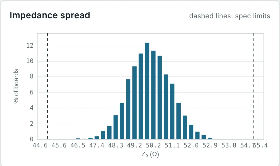
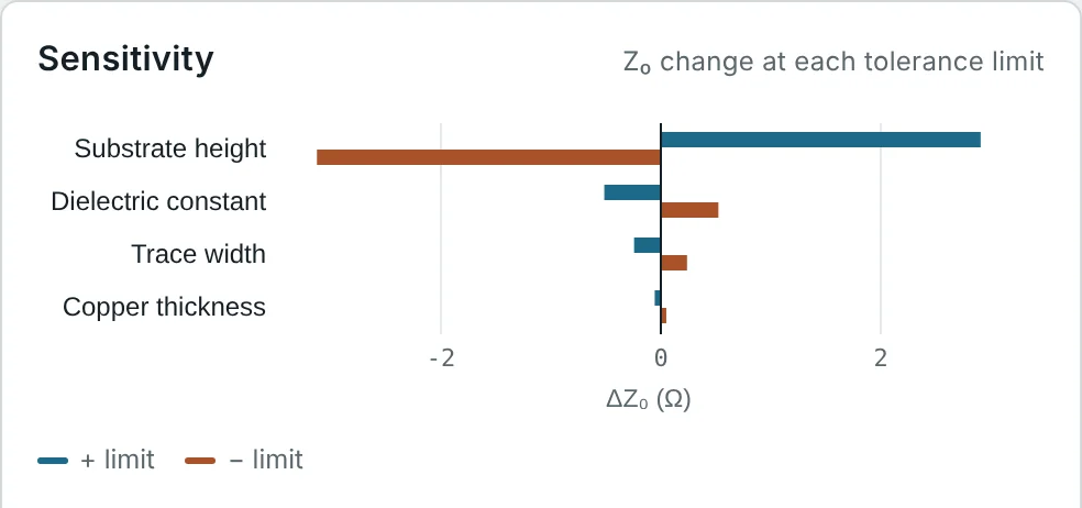
The last point is critical for PCB design. Fig 3 shows a Monte Carlo analysis from the microstrip calculator for the 50 Ω FR-4 line, with typical fabrication tolerances: trace width ±25 µm, substrate height ±10%, εr ±0.10 and copper thickness ±5 µm. The impedance spread has a standard deviation of 1.0 Ω (±3σ = ±6%), and the sensitivity chart shows that the substrate height dominates — a 10% thickness change moves Z₀ by about 3 Ω, six times more than the dielectric-constant tolerance. This is why fabricators sell "controlled impedance" boards with a ±10% or ±5% specification and adjust the etched width to compensate for the laminate actually used.
Characteristic Impedance vs Load Impedance
Z₀ belongs to the line; the load impedance ZL belongs to whatever is connected at the end. Their relationship decides what happens to the wave at the load, through the reflection coefficient:
Three consequences are worth separating clearly:
- The impedance seen at the input depends on Z₀, ZL and the electrical length — unless ZL = Z₀, in which case it is Z₀ at every length and every frequency. That is the practical meaning of "matched": a matched line is invisible.
- A mismatch costs power (mismatch loss ML) and, on a transmitter, can damage the output stage through high VSWR.
- Z₀ itself can be any value — a 75 Ω line is just as good as a 50 Ω line if the source and load are 75 Ω. Problems arise only at the boundaries between different impedances, including connectors and changes of line width (Part 13).
Mismatches and their correction are the subject of the Smith chart series; Part 7 derives the input impedance of a terminated line.
Measuring Characteristic Impedance
Because Z₀ is not a resistance, it is measured indirectly. Three methods are common:
Measure the input impedance of a length ℓ of lossless line twice, once with the far end short-circuited and once open. From the input-impedance formula of Part 7 with ZL = 0 and ZL = ∞:
Their product removes the length dependence, and their ratio gives the electrical length:
- Time-domain reflectometry (TDR). Launch a fast step from a known Zs (usually 50 Ω) and measure the reflected step. Each section of line shows up at a delay set by its position, with Γ = (Z₀ − Zs)/(Z₀ + Zs). TDR is the standard way PCB fabricators verify controlled-impedance coupons.
- Capacitance and delay. Z₀ = τ/C for a length of line, with C measured at low frequency and τ from a pulse or the frequency of the first quarter-wave resonance.
- Vector network analyser. Measure S-parameters of a line section and extract Z₀ and γ from them — the most accurate method at microwave frequencies.
Practical Characteristic Impedance Calculations
The worked examples below use c = 2.998 × 10⁸ m/s and η₀ = 376.7 Ω.
Identifying an Unknown Cable from C and Delay
Problem: A 1.00 m length of unmarked coax measures 67 pF between its conductors, and a pulse takes 5.05 ns to travel through it. Find Z₀, L′ and the velocity factor.
RG-59 and RG-6 with solid PE match this description. The method needs no RF equipment — a capacitance meter and an oscilloscope suffice.
Lossy Z₀ of RG-58 at Low Frequency
Problem: RG-58 has L′ = 258.5 nH/m, C′ = 96.8 pF/m and a DC loop resistance of 0.045 Ω/m. Find Z₀ at 1 kHz and at 100 kHz (R′ = 0.061 Ω/m including skin effect).
"50 Ω" cable is 50 Ω only at RF. An audio engineer driving a long coax run, or a designer of a DC-to-GHz instrument, must allow for the complex low-frequency Z₀ shown in Fig 2.
The Imaginary Part of Z₀ on a Low-Loss Line
Problem: The coax of Part 3, Example 1 has R′ = 0.8 Ω/m, L′ = 250 nH/m, G′ = 0.1 mS/m and C′ = 100 pF/m. Use the low-loss formula to find Z₀ at 1 GHz.
Because R′/L′ > G′/C′ (conductor loss dominates), the small imaginary part is negative (capacitive). Adding a little loading inductance, or a little dielectric loss, would move the line towards Heaviside's distortionless condition and make it zero.
Measuring Z₀ with Open and Short Terminations
Problem: A VNA measures a length of cable at 100 MHz as Zsc = j35.1 Ω with the far end shorted and Zoc = −j71.2 Ω with it open. Find Z₀ and the electrical length.
The ambiguity of n × 180° is resolved by repeating the measurement at a slightly different frequency or from the approximate physical length. The method works with any impedance analyser and needs no 50 Ω reference.
Designing a 75 Ω Foam Coax
Problem: A 75 Ω satellite-TV cable uses gas-injected foam PE (εr = 1.5) and a 1.0 mm diameter centre conductor. What diameter must the foam dielectric be?
RG-6 satellite cable has a 1.0 mm centre conductor and a 4.6–4.7 mm foam dielectric — exactly this. With solid PE (εr = 2.25) the dielectric would have to be 6.5 mm across for the same 75 Ω, which is why foam both lowers the loss and shrinks the cable.
Impedance Tolerance of a 50 Ω FR-4 Trace
Problem: For the 3.07 mm, 50 Ω microstrip on 1.6 mm FR-4 (35 µm copper), estimate Z₀ at the limits of (a) ±50 µm etch tolerance, (b) εr = 4.1–4.5 and (c) ±10% substrate height. Which matters most?
On a thick board with wide traces the dielectric height and εr dominate; on thin boards with narrow traces the etch tolerance becomes the largest term. Matching Fig 3b, the first item on a controlled-impedance specification should be the dielectric thickness between the trace and its reference plane.
Spacing of a 300 Ω Twin-Lead
Problem: What centre spacing D gives 300 Ω for two 1.0 mm diameter wires in air? How does a polyethylene web that raises εeff to 1.3 change the impedance?
Commercial 300 Ω ribbon uses a wider spacing (about 8–10 mm for thinner wire) to compensate for the web. Moisture on the web raises εeff further — the reason twin-lead's impedance drifts in rain.
Connecting a 75 Ω Device to a 50 Ω System
Problem: A 75 Ω video receiver is connected to a 50 Ω generator through 50 Ω cable. Find Γ, the return loss, the VSWR and the mismatch loss.
Only 4% of the power is reflected, so for many purposes a 50/75 Ω mismatch is tolerable. For precision measurements a minimum-loss matching pad (5.7 dB loss) is used instead.
Why a Matched Line Is Invisible
Problem: A 10 m, 50 Ω line is terminated (a) in 50 Ω and (b) in 75 Ω. Between what limits can the input impedance lie as the frequency (and so the electrical length) varies?
With a matched load the line has no effect on the impedance, so any length can be used. With a mismatch the source sees an impedance that depends on cable length and frequency — the reason that cable length "matters" only in mismatched systems.
Measuring a PCB Coupon by TDR
Problem: A TDR with a 50 Ω source launches a 250 mV step into a PCB test coupon. The reflection from the coupon trace is a +27 mV step. What is the trace impedance? Is it within a 50 Ω ± 10% specification?
The trace is about 24% high, typically caused by a thinner-than-specified trace or a thicker dielectric. Fabricators make exactly this measurement on a coupon at the edge of each panel and adjust the etch compensation until the coupons pass.
Summary
- Z₀ is the voltage-to-current ratio of a single travelling wave, and the input impedance of an infinite line or of any line terminated in Z₀.
- From the infinite ladder: Z₀ = √((R′ + jωL′)/(G′ + jωC′)). Lossless: Z₀ = √(L′/C′), real and frequency-independent.
- Low-loss: Z₀ ≈ √(L′/C′)[1 − (j/2ω)(R′/L′ − G′/C′)]. At low frequency Z₀ → √(R′/jωC′), with an angle near −45°.
- Z₀ = vpL′ = 1/(vpC′) = τ/C; L′ = Z₀√εeff/c and C′ = √εeff/(cZ₀).
- 50 Ω is the compromise between the 30 Ω power optimum and the 77 Ω loss optimum of air coax; 75 Ω is used where loss matters most.
- Z₀ is set by geometry and εr; on PCBs the dielectric thickness usually dominates its tolerance.
- Measure Z₀ with Z₀ = √(ZocZsc), with TDR, or from capacitance and delay.
Z₀ describes the relation between voltage and current in a wave; the propagation constant describes how the wave itself changes as it travels. Part 5: Propagation Constant, Phase Velocity and Group Velocity examines γ in detail — attenuation, phase constant, phase and group velocity, and dispersion.
Every point on the Smith chart is an impedance normalised to Z₀ — the chart only works once Z₀ is known. Open Smith Chart & Impedance Matching series →
Put It Into Practice
Use the NEXT ANTENNAS calculators to apply the ideas from this article to real lines and circuits.