Why Passive Components Behave Differently at RF
At low frequencies a resistor resists, a capacitor stores charge, and an inductor stores magnetic energy — each behaves almost exactly as its ideal circuit model predicts. At radio frequencies the picture changes completely. Every physical component has parasitic elements — unavoidable stray inductance, capacitance, and resistance introduced by the package leads, bond wires, electrode geometry, and the dielectric or magnetic core material.
These parasitics are negligible at 50 Hz. At 1 GHz they can dominate the component's behaviour entirely, turning a capacitor into an inductor, a resistor into a resonator, or a bypass capacitor into an open circuit. Understanding this is not an academic exercise — it is the difference between a working RF circuit and one that fails mysteriously on the bench.
Always specify the operating frequency alongside the component value. A "100 nF bypass capacitor" is meaningless without knowing the frequency — at 1 MHz it bypasses well; at 500 MHz it may present a net inductive impedance and do the opposite of what is intended.
Resistors at Low and High Frequency
The Ideal Resistor
An ideal resistor has impedance Z = R at all frequencies — purely real, frequency-independent. Real resistors depart significantly from this as frequency increases.
Parasitic Model of a Real Resistor
A physical resistor — whether through-hole or surface-mount — has three parasitic elements that become significant at RF:
- Lead/pad inductance (Ls): The resistance element connects to pads or leads through conductors. Any conductor has inductance. For a 0402 SMD resistor, Ls ≈ 0.3–1 nH.
- Shunt capacitance (Cp): The resistive element and its electrodes form a capacitor across the component. For a 0402 SMD resistor, Cp ≈ 0.05–0.1 pF.
- Skin effect resistance: At high frequencies, current flows only in the skin of the conductors, increasing the effective series resistance.
The complete impedance of a real resistor with series inductance Ls and shunt capacitance Cp is:
Resistor Impedance vs Frequency
Three distinct frequency regions define resistor behaviour:
- Low frequency (resistive region): Z ≈ R. The component behaves as intended.
- Mid frequency (inductive region): The series inductance Ls begins to dominate. |Z| rises above R. The component behaves like a series RL network.
- High frequency (resonant/capacitive region): Ls and Cp form a parallel resonance at fres = 1/(2π√(LsCp)). Above resonance, Cp dominates and |Z| falls — the resistor behaves capacitively.
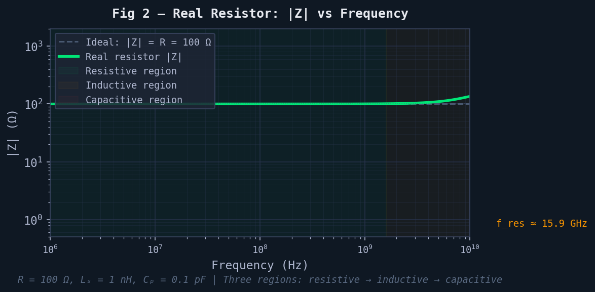
A 50 Ω termination resistor used for broadband matching above 3 GHz may no longer present 50 Ω — its inductive parasitics can shift the impedance significantly. Always verify with S-parameter data (Touchstone files) from the manufacturer above 1 GHz. Smaller packages (0402, 0201) have lower parasitics and are preferred at microwave frequencies.
Resistor Technologies at RF
- Thin-film SMD (0402, 0201): Best RF performance. Low parasitics, tight tolerance (0.1%), low temperature coefficient. Preferred for RF attenuators, matching networks, and bias networks above 1 GHz.
- Thick-film SMD: Higher parasitics, lower cost. Adequate for RF below 500 MHz.
- Wirewound: Extremely high inductance — avoid at any RF frequency. The inductive reactance completely dominates above a few MHz.
- Carbon film through-hole: Poor RF performance due to long lead inductance. Generally avoid above 10 MHz.
Capacitors at Low and High Frequency
The Ideal Capacitor
An ideal capacitor has impedance that falls with increasing frequency:
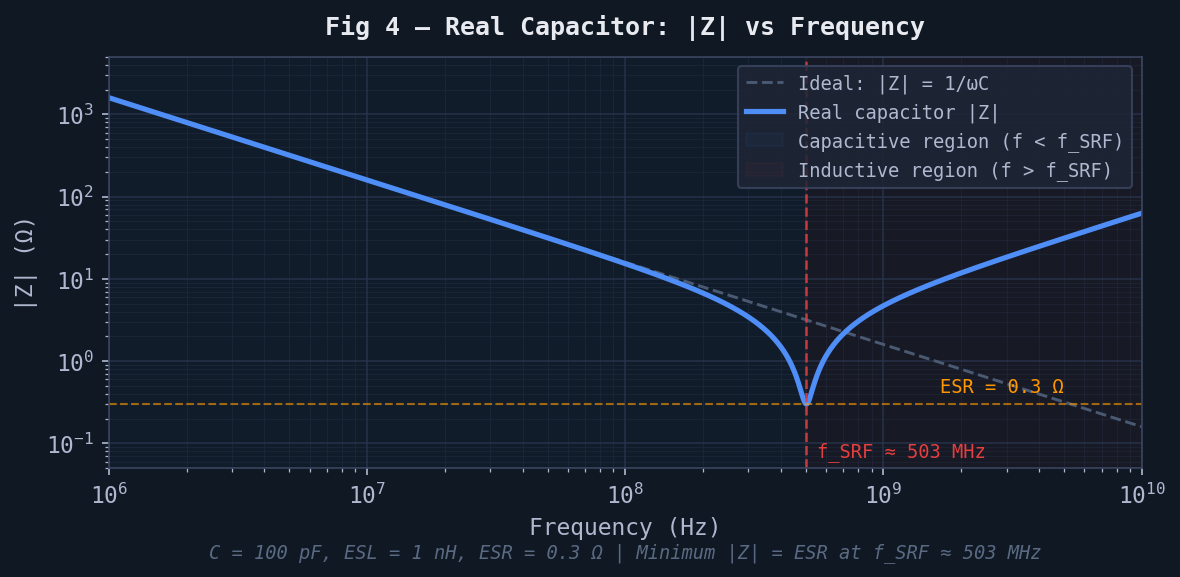
This is the ideal picture. A real capacitor behaves this way only over a limited frequency range, bounded by its self-resonant frequency (SRF).
Parasitic Model — The Real Capacitor
Every physical capacitor has three parasitic elements:
- Equivalent Series Resistance (ESR): Resistive losses in the electrode material, leads, and dielectric. Causes heating and limits Q factor. For a 100 pF MLCC at 1 GHz, ESR ≈ 0.1–0.5 Ω.
- Equivalent Series Inductance (ESL): Inductance of the leads, bond wires, and electrodes. For a 0402 MLCC, ESL ≈ 0.3–1 nH. This is the dominant limiting parasitic at RF.
- Equivalent Parallel Resistance (EPR): Leakage resistance across the dielectric — usually very large (MΩ to GΩ) and negligible at RF.
Self-Resonant Frequency (SRF)
The series combination of ESL and C forms a series resonance at the self-resonant frequency. At the SRF, the capacitor presents its minimum impedance (equal to ESR alone). Above the SRF, the ESL dominates and the component behaves as an inductor — its impedance rises with frequency:
Q Factor of a Capacitor
The quality factor Q measures the ratio of energy stored to energy dissipated per cycle. For a capacitor, Q is dominated by ESR:
Capacitor Technologies at RF
- MLCC (Multi-Layer Ceramic Capacitor), C0G/NP0: Best RF capacitor. Stable capacitance vs temperature and voltage, very low ESR and ESL, Q > 1000 at 1 MHz. Essential for RF coupling, bypassing, and matching networks above 100 MHz.
- MLCC X7R/X5R: Capacitance varies with DC bias (up to −80% at rated voltage) and temperature. Acceptable for bypass below 500 MHz; avoid in precision RF matching.
- Electrolytic (aluminium, tantalum): Very high ESL and ESR. Self-resonant at 1–10 MHz. Useful only for low-frequency power supply bypassing — never for RF signal paths.
- Film (polyester, polypropylene): Good stability but large physical size increases parasitics. Used for audio and power electronics, rarely in RF above 50 MHz.
For RF power supply bypassing, never rely on a single large capacitor. Use a parallel combination: 100 nF (C0G) for mid-range bypass + 10 pF (C0G) for high-frequency bypass. The smaller capacitor has a higher SRF and handles GHz bypassing; the larger capacitor handles lower frequencies. Place them as close as possible to the device VCC pin with short, wide traces to ground.
Inductors at Low and High Frequency
The Ideal Inductor
An ideal inductor has impedance that rises linearly with frequency:
Parasitic Model — The Real Inductor
A physical inductor — whether a chip inductor, air-core coil, or toroid — has three significant parasitic elements:
- Series DC resistance (RDC): Resistance of the wire forming the coil. Always present. Limits Q at low frequencies.
- Series AC resistance (RAC): Skin effect and proximity effect increase winding resistance with frequency. RAC ∝ √f.
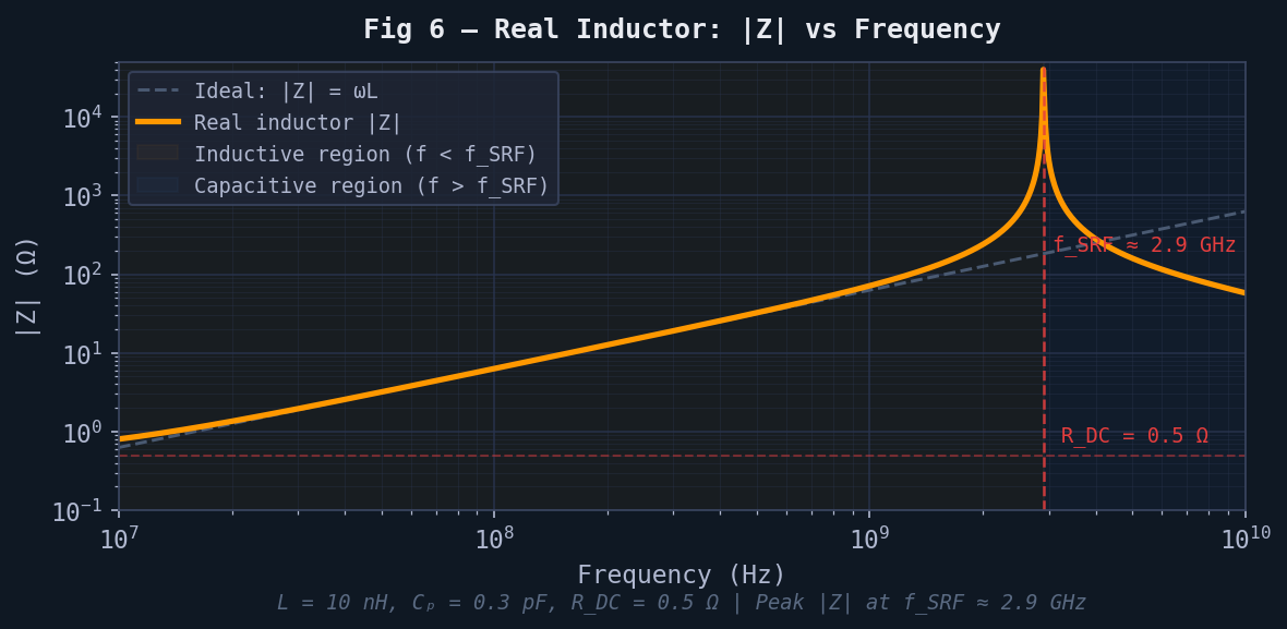
- Shunt capacitance (Cp): Inter-winding capacitance between adjacent turns. This is the dominant RF parasitic — it forms a parallel resonance with the inductance, creating the SRF above which the component behaves as a capacitor.
- Core losses: Magnetic core materials (ferrite) have frequency-dependent permeability and loss. Above the core's useful frequency range, permeability collapses and loss increases sharply.
Self-Resonant Frequency and Q Factor
The parallel resonance between L and Cp produces the inductor's SRF. At the SRF, impedance is maximum (theoretically infinite for a lossless inductor, in practice limited by winding resistance). Above the SRF, Cp dominates — the component behaves as a capacitor:
Inductor Technologies at RF
- Air-core solenoid / loop: No core losses, highest Q possible. SRF can be very high. Used in VHF/UHF matching networks and filters. Self-supporting or wound on non-magnetic former. Q = 100–400 at 100 MHz is achievable.
- Chip inductor (ferrite core, 0402): Compact, low cost. Core permeability collapses above a few hundred MHz for most ferrites. Useful up to ~3 GHz for small values (1–10 nH). Always verify SRF and Q vs frequency from manufacturer S-parameter data.
- Bondwire / printed spiral: At mmWave frequencies, the parasitic inductance of bond wires and PCB traces IS the inductor. A 1 mm bond wire ≈ 1 nH. PCB microstrip stubs can realise inductances at GHz.
- Toroid (ferrite): High inductance density, low EMI leakage. Permeability falls sharply above material's rated frequency. Not used at microwave frequencies.
Above the SRF, the component is capacitive — using it as a "choke" or "RF block" above its SRF will do the opposite: it will pass high-frequency signals rather than block them. Always select inductors with SRF at least 2–3× above your highest operating frequency, and verify with the manufacturer's S-parameter data.
Comparison — All Three Components
The table below summarises how each component type behaves across three frequency regions, and the transition that occurs at the SRF:
| Component | Low Frequency | Near SRF | Above SRF | Key Parasitic |
|---|---|---|---|---|
| Resistor | Z ≈ R ✓ | Z rises (inductive) | Z falls (capacitive) | Lₛ, Cₚ |
| Capacitor | Z = 1/ωC ↓ ✓ | Z → ESR (min) | Z rises (inductive!) | ESL, ESR |
| Inductor | Z = jωL ↑ ✓ | Z → ∞ (max) | Z falls (capacitive!) | Cₚ, R_AC |
Practical Design Guidelines
- Always verify S-parameters. Never rely on a component's nominal value alone above 100 MHz. Download the manufacturer's S2P Touchstone file and simulate the actual component behaviour in your circuit simulator (AWR, ADS, Qucs-S, or RFSim99).
- Use the smallest package you can solder. 0402 has lower parasitics than 0805; 0201 is lower still. At 5 GHz+, 0201 is the practical minimum for SMD components.
- Operate below 50% of the SRF. The component behaves approximately as intended below half its SRF. Above this, parasitics cause significant deviation from the nominal model.
- Specify C0G/NP0 dielectric for RF capacitors. Never use X7R or Y5V in a matching network or RF filter — capacitance shifts with voltage and temperature.
- Treat the PCB as part of the component. Pad size, trace length to ground, via inductance, and ground plane proximity all modify the effective component impedance. Via inductance ≈ 0.3–1 nH per via.
- Keep RF ground return paths short. The ground return is in series with every shunt component. A long PCB trace to ground adds inductance that defeats bypass capacitors and shifts resonances.
Worked Examples — 5 Calculations
Apply the equations from this article to real-world RF component problems. Each example walks through the full calculation step by step.
Self-Resonant Frequency of a Bypass Capacitor
Problem: A 100 nF MLCC bypass capacitor has an equivalent series inductance (ESL) of 0.8 nH. At what frequency does this capacitor self-resonate? Is it still useful as a bypass at 1 GHz?
At 1 GHz, this capacitor is operating at 56× above its SRF. It behaves as an inductor with impedance |Z| = ω·ESL − 1/(ωC) ≈ ω·ESL ≈ 2π×10⁹×0.8×10⁻⁹ ≈ 5 Ω — providing inductance, not bypassing. Replace with a 10 pF C0G capacitor (SRF ≈ 1–2 GHz) in parallel.
Inductive Reactance of a 51 Ω Resistor at 2.4 GHz
Problem: A 0402 51 Ω thin-film resistor has a lead inductance Ls = 0.5 nH and a shunt capacitance Cp = 0.05 pF. Calculate the actual impedance magnitude |Z| at 2.4 GHz. How much does it deviate from 51 Ω?
The 0402 thin-film performs well at 2.4 GHz — the inductive reactance jωLₛ = j7.54 Ω adds only a small imaginary component. The magnitude error is ~1%, which is acceptable. The phase angle is arctan(7.54/51) ≈ 8.4° — enough to matter in precision networks but acceptable in bias resistors. A 0201 package would have Lₛ ≈ 0.3 nH, giving an even smaller error.
Q Factor of a Chip Capacitor at 500 MHz
Problem: A 22 pF C0G MLCC capacitor has ESR = 0.15 Ω at 500 MHz. Calculate its Q factor at this frequency. Is this adequate for a 500 MHz bandpass filter?
Q = 97 is a high-quality capacitor for 500 MHz. Bandpass filter design typically requires component Q of at least 10–20× the circuit Q. For a filter with 1% fractional bandwidth (circuit Q = 100), component Q = 97 would be marginal — use a capacitor with ESR ≤ 0.1 Ω for this application. C0G capacitors consistently deliver Q > 100 at VHF/UHF, which is why they are the only acceptable choice for RF filter capacitors.
Inductor Q and SRF — Choosing Between Two Chip Inductors
Problem: You need a 10 nH inductor for a 1.5 GHz matching network. Two options are available: Inductor A: L = 10 nH, SRF = 3.0 GHz, RDC = 0.35 Ω. Inductor B: L = 10 nH, SRF = 8.0 GHz, RDC = 0.80 Ω. Calculate Q at 1.5 GHz for each and decide which to use.
Inductor A has higher Q (lower loss) but its SRF = 3.0 GHz is only 2× above 1.5 GHz — below the recommended 3× safety margin. At 1.5 GHz it operates at 50% of its SRF, where capacitive parasitics already cause the effective inductance to deviate from the nominal 10 nH value. Inductor B has lower Q but SRF = 8 GHz gives 5.3× margin — the inductance is far more stable and predictable at 1.5 GHz. In practice, choose Inductor B — stable inductance and predictable behaviour matters more than raw Q in a matching network.
Parallel Bypass Capacitor Strategy — What Frequency Does Each Capacitor Handle?
Problem: A 5 GHz LNA requires power supply bypassing. Two C0G capacitors are placed in parallel: C1 = 100 pF (ESL = 0.8 nH) and C2 = 10 pF (ESL = 0.5 nH). Calculate the SRF of each, identify which capacitor handles each frequency range, and determine whether bypassing is adequate at 5 GHz.
C₁ handles DC–562 MHz. C₂ handles 562 MHz–2.25 GHz. Above 2.25 GHz, both capacitors are inductive and neither provides effective bypassing. At 5 GHz a third capacitor is needed — a 1–2 pF C0G (SRF ≈ 4–6 GHz) placed as close as possible to the LNA VCC pin with the shortest possible ground via. This three-capacitor strategy ensures effective bypassing from DC to well above 5 GHz.