Coplanar Waveguide (CPW) Calculator

Free CPW impedance calculator using conformal mapping with elliptic integrals. Enter signal conductor width, slot gap, and substrate — instantly get characteristic impedance Z₀, effective permittivity εeff, phase velocity, and guided wavelength. Interactive slider controls update the live cross-section diagram in real time.

Coplanar waveguide — structure & field distribution
A CPW places the signal conductor and both ground planes on the same surface of the substrate. The signal conductor of width w is flanked by two symmetric slots of width g, beyond which lie the ground planes. The substrate has thickness h and relative permittivity εr. The field is confined primarily in the two slots, allowing surface-mount probing without vias.
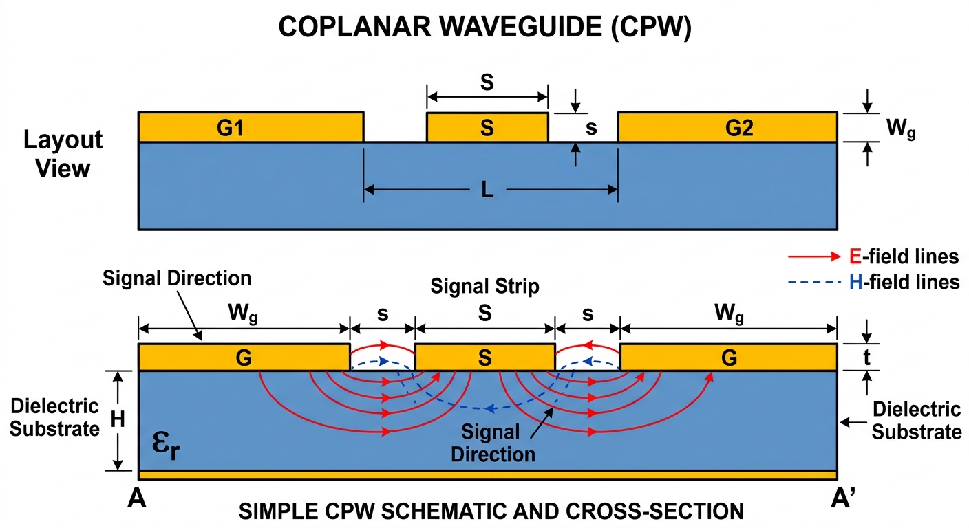
Coplanar waveguide CPW cross-section showing signal conductor, slot gaps, ground planes, dielectric substrate, and electric and magnetic field distributions
k = w/(w+2g) = 0.600 Quasi-TEM Mode Coplanar Line
Dielectric Substrate (εr = 4.4, h = 1.60 mm) Back ground plane GND W GND g = 0.50 mm w = 1.50 mm g = 0.50 mm
1.50 mm
0.50 mm
Substrate
Relative permittivity εr
Substrate thickness h (mm)
Conductor thickness t (mm)
Common substrates
Editing εr / h / t clears the preset selection.
CPW geometry
Signal conductor width w (mm)
Slot gap width g (mm)
Target Z₀ presets
Frequency f (GHz)
Results
Signal width w
—
mm
Slot gap g
—
mm
Fill ratio k = w/(w+2g)
—
dimensionless
Characteristic Z₀
—
Ω
Effective εeff
—
εeff
Phase velocity
—
×10⁸ m/s
Guided wavelength
λg (full wave)
—
mm
λg / 2
—
mm
λg / 4
—
mm
Additional outputs
Wave number β
—
rad/m
Free-space λ₀
—
mm at freq
Slowdown factor
—
vp / c
GHz
λg = vp / f = (c / √εeff) / f  ·  β = 2π / λg
⚠ Geometry outside typical range — verify with EM simulation.
Method & reference

Uses conformal mapping with complete elliptic integrals K(k) computed via the arithmetic-geometric mean (AGM) algorithm — equivalent to full numerical integration, converging in under 20 iterations. The finite-substrate correction is applied through a modified fill ratio using hyperbolic functions of w, g, and h. Conductor thickness correction follows Schneider's approximation when t > 0. Valid for h ≫ g and w/h > 0.1.

Reference: Ghione & Naldi, IEEE Trans. MTT, 1987. Also: Simons, Coplanar Waveguide Circuits, Components, and Systems, Wiley 2001.

📐 Design your antenna Patch Antenna Calculator Compute patch width, length, inset feed depth, and notch gap for any substrate and frequency.  → 〰️ Compare transmission lines Microstrip Width Calculator Compute microstrip trace width, εeff, phase velocity, and guided wavelength using Hammerstad–Jensen synthesis.  →

What Is a Coplanar Waveguide?

A coplanar waveguide (CPW) is a planar transmission line in which the signal conductor and both return ground planes lie on the same surface of the substrate. Invented by C. P. Wen in 1969, CPW is now the dominant transmission line format for MMICs, millimetre-wave probes, and high-speed PCB interconnects because the ground reference is always accessible from the top surface without requiring via holes through the substrate.

Key advantages over microstrip

  • Same-layer ground access — shunt components connect to ground without vias, eliminating parasitic via inductance
  • Ground-signal-ground (GSG) probing — on-wafer and on-board RF probes land directly on the CPW pattern
  • Impedance set by the w/g ratio — independent of substrate thickness, enabling compact designs on any dielectric
  • Lower dispersion at mm-wave — field confined in the slots rather than the full substrate thickness
  • Flip-chip and wire-bond compatible — all interconnects on a single surface layer

Design Variables

SymbolNameTypical range
wSignal conductor width0.1 – 5 mm
gSlot gap width0.05 – 2 mm
hSubstrate thickness0.127 – 3.175 mm
εrRelative permittivity2.1 – 12
tConductor thickness5 μm – 70 μm
kFill ratio w / (w + 2g)0 – 1 (dimensionless)

Characteristic Impedance — Conformal Mapping

The CPW cross-section is mapped conformally to a parallel-plate capacitor via the Schwarz–Christoffel transformation. The result expresses Z₀ as a ratio of complete elliptic integrals of the first kind K(k).

Fill ratio k (infinite substrate)
k = w w + 2g ,   k' = √(1 − k²)
w = signal conductor width · g = slot gap · k → 1 means very wide conductor (low Z₀) · k → 0 means narrow conductor (high Z₀)
Finite substrate correction — fill ratio k₁
k₁ = sinh(πw / 4h) sinh(π(w + 2g) / 4h) ,   k₁' = √(1 − k₁²)
h = substrate thickness · as h → ∞, k₁ → k (recovers the infinite-substrate case)
Effective permittivity εeff
εeff = 1 + εr − 1 2 · K(k₁') · K(k) K(k₁) · K(k')
K(k) = complete elliptic integral of the first kind · the substrate filling factor weights εr against unity
Characteristic impedance Z₀
Z₀ = 30π √εeff · K(k') K(k)
For 50 Ω on FR-4 (εr = 4.4, h = 1.6 mm): typical starting point is w = 1.5 mm, g = 0.5 mm

Elliptic Integral — AGM Algorithm

K(k) has no closed-form expression but converges rapidly using the arithmetic-geometric mean (AGM):

AGM algorithm for K(k)
a₀ = 1,   b₀ = k' = √(1 − k²)
aₙ₊₁ = aₙ + bₙ2 ,   bₙ₊₁ = √(aₙ · bₙ)
K(k) = π2 · a∞  (a∞ = AGM limit, converges in ~15 iterations)

CPW vs Microstrip

PropertyCPWMicrostrip
Ground reference layerSame surface as signalOpposite surface
Via holes for shunt elementsNot requiredRequired
GSG RF probe landingDirectRequires adaptation
Impedance control parameterw/g ratiow/h ratio
Substrate thickness dependenceWeak (finite h correction only)Strong
mm-wave dispersionLowerHigher
Radiation / leakage at low freqHigherLower
50 Ω starting point on FR-4 (εr = 4.4, h = 1.6 mm): Set signal width w = 1.5 mm and slot gap g = 0.5 mm. The fill ratio k = w/(w+2g) = 0.60 yields Z₀ ≈ 50 Ω. To increase Z₀, widen the slots (larger g) or narrow the signal conductor (smaller w). To decrease Z₀, do the opposite. The ground plane extent beyond each slot should be at least 5× the slot gap to approximate an infinite ground plane.

If your design uses microstrip rather than CPW — or if you need to transition between the two on the same board — use our Microstrip Width Calculator to compute the equivalent 50 Ω trace width, effective permittivity, and guided wavelength for your substrate. Both tools use the same substrate presets, so you can compare results side by side.

〰️ Single-sided ground plane alternative Microstrip Width Calculator Hammerstad–Jensen synthesis for trace width W, εeff, phase velocity, and guided wavelength — same substrates, instant results.  →

More RF Transmission Line Tools

Explore our full suite of free RF calculators — microstrip width, patch antenna, noise figure, Smith chart, and more.